


 |
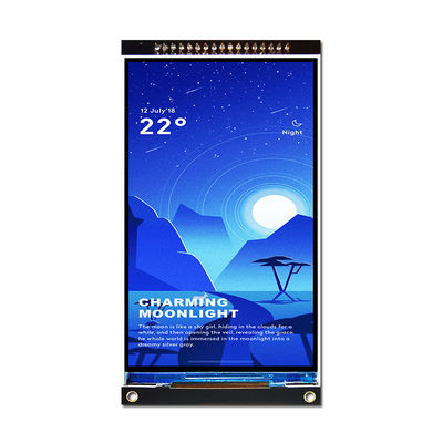
Sunlight Readable TFT LCD Module 4.3 Inch 480x800 NT35510 TFT_H043A4WVIST5N60
Product Details:
| Place of Origin: | dongguan,China |
| Brand Name: | HOTHMI |
| Model Number: | TFT-H043A4WVIST5N60 |
Payment & Shipping Terms:
| Minimum Order Quantity: | 2 |
|---|---|
| Delivery Time: | 25 days |
| Payment Terms: | L/C, D/A, T/T, D/P, Western Union, MoneyGram |
| Supply Ability: | 99999 |
|
Detail Information |
|||
| Product Type: | TFT Module | Display Size: | 4.3 Inches |
|---|---|---|---|
| Display Content: | 480x800 Dots | Interface: | MCU / RGB / MIPI / MDDI |
| Working Temperature: | -20~70℃ | Driver Chip Model: | NT35510 |
| High Light: | Sunlight Readable TFT LCD Module,MCU TFT LCD Module,MDDI TFT LCD Display Module |
||
Product Description
4.3 Inch 480x800 Sunlight Readable TFT Display Module NT35510/TFT_H043A4WVIST5N60
Product parameters
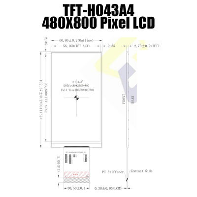
Dimensions (mm) - 60.86x104.50x 2.50
Effective size mm - 56.16x93.60
Product Application - Handheld Instruments
Angle - Full Angle
Backlight type or brightness - 500cd/m2
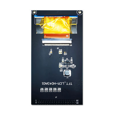
Connection method PIN number - FPC-60PIN
Supply voltage - 3.3v
General Feature
| Item | Standard Value | Unit |
| Display Size | 4.3” | -- |
| Number of Pixels | 480(H)x3(RGB)*800(V) | -- |
| Active Area | 56.16(H) *93.60(V) | mm |
| LCM Outline Dimension | 60.86(H) ×102.57× 2.70(V) | mm |
| Viewing Direction | Full O’Clock | - |
| LCM Interface | With CPU / RGB / MIPI / MDDI Interface | - |
| LCM Driver IC | NT35510 | - |
| LCM Driver Voltage | IOVCC=1.8V,VCI=3.3V (Typ) | V |
| Backlight | White LED | - |
| Touch Panel | Without Touch Panel | - |
| CTP Driver IC | - - - | - |
| CTP Driver Voltage | - - - | V |
| CTP I/O Digital Voltage | - - - | V |
| Operation Temperature | -20~70 | ℃ |
| Storage Temperature | -30~80 | ℃ |
Pin Description
| Pin NO. | Symbol | Description |
| 1,2 | GND | Ground |
|
3 |
D0N |
♦These pins are DSI-D0+/- differential data signals if MIPI interface is used. ♦These pins are MDDI_DATA0_P/M differential strobe signals if MDDI interface is used. ♦If not used, please fix this pin at GND. |
|
5 |
D0P |
|
| 5,6 | GND | Ground |
|
7 |
DCLKN |
♦These pins are DSI-CLK+/- differential clock signals if MIPI interface is used. ♦These pins are MDDI_STB_P/M differential strobe signals if MDDI interface is used. ♦If not used, please fix this pin at GND. |
|
8 |
DCLKP |
|
| 9 | GND | Ground |
|
10 |
D1N |
♦These pins are DSI-D1+/- differential data signals if MIPI interface is used. ♦These pins are MDDI_DATA1_P/M differential strobe signals if MDDI interface is used. ♦If not used, please fix this pin at GND. |
|
11 |
D1P |
|
| 12 | GND | Ground |
| 13 | VCI | Analog Power |
| 14 | IOVCC | Power supply for interface system |
| 15 | VSD |
♦ Vertical synchronizing input signal for RGB interface. ♦ If not used, please fix this pin at GND. |
| 16 | HSD |
♦ Horizontal synchronizing input signal for RGB interface. ♦ If not used, please fix this pin at GND. |
| 17 | PCLK |
♦ Pixel clock signal for RGB interface. ♦ If not used, please fix this pin at GND. |
| 18 | DEN |
♦ Data enable signal for RGB interface. ♦ If not used, please fix this pin at GND. |
|
19-42 |
DB0-DB23 |
♦ Data Bus. ♦ If not used, please fix this pin at GND. |
| 43 | RESET | LCM Reset Pin. |
|
44 |
CSX |
♦ Chip select input pin (“Low” enable) in 80-series MPU I/F and SPI I/F. ♦ This pin is not used for MIPI or MDDI I/F, please fix this pin at GND. |
| 45 | RDX |
♦ Read enable in 8080 MCU parallel IF. Low-active. ♦If not used, please fix this pin at GND. |
|
46 |
WRX |
♦ Write enable in MCU parallel interface ♦ In SPI mode, this pin is used as SCL. ♦ In I2C mode, Serial input clock in I2C I/F ♦ If not used, please fix this pin at GND. |
| 47 | DCX |
♦ Display data/command selection pin in parallel IF. ♦ If not used, please fix this pin at GND. |
|
48 |
SPI_SDI |
♦ In SPI mode,SPI interface input/output pin. ♦ In I2C mode, Serial input/output signal in I2C I/F. ♦ If not used, please fix this pin at GND. |
| 49 | SPI_SDO |
♦ In SPI mode,SPI interface output pin. ♦ If not used, please let this pin open. |
|
50 |
TE |
♦ Tearing effect signal is used to synchronize MCU to frame memory writing. ♦ If not used, please let this pin open. |
| 51-54 | IM0-IM3 | The MCU interface mode select |
|
55 |
PSWAP |
♦ Input pin to select HSSI_D0/D1 data lane sequence and polarity in high speed interface only. ♦ For MIPI interface, both DSWAP and PSWAP function are available. ♦ For MDDI interface, only PSWAP function is available. i.e. DSWAP=1 in below table is invalid. ♦ If not used, please fix this pin at GND. |
|
56 |
DSWAP |
|
|
57 |
LANSEL |
♦ Input pin to select 1 data lane or 2 data lanes in MIPI/MDDI interface. ♦ If not used, please fix this pin at GND. |
| 58 | MTP | No Conect |
| 59 | LED_A | LED Anode |
| 60 | LED_K | LED Cathode |
Search keyword: tft 4.3, tft 4.3", 4.3 tft lcd, 4.3" tft lcd, 4.3 inch tft lcd, tft lcd 4.3, 4.3 tft display, 4.3" tft display, 4.3 inch tft display, tft display 4.3, tft display 4.3"
![]()
![]()
![]()
![]()
![]()
![]()
![]()
![]()
![]()