-300x300.jpg)
Description
Product Description and Core Highlights of the LVDS Screen
Detailed Introduction of LVDS Screen
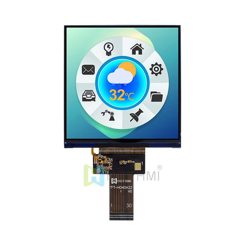
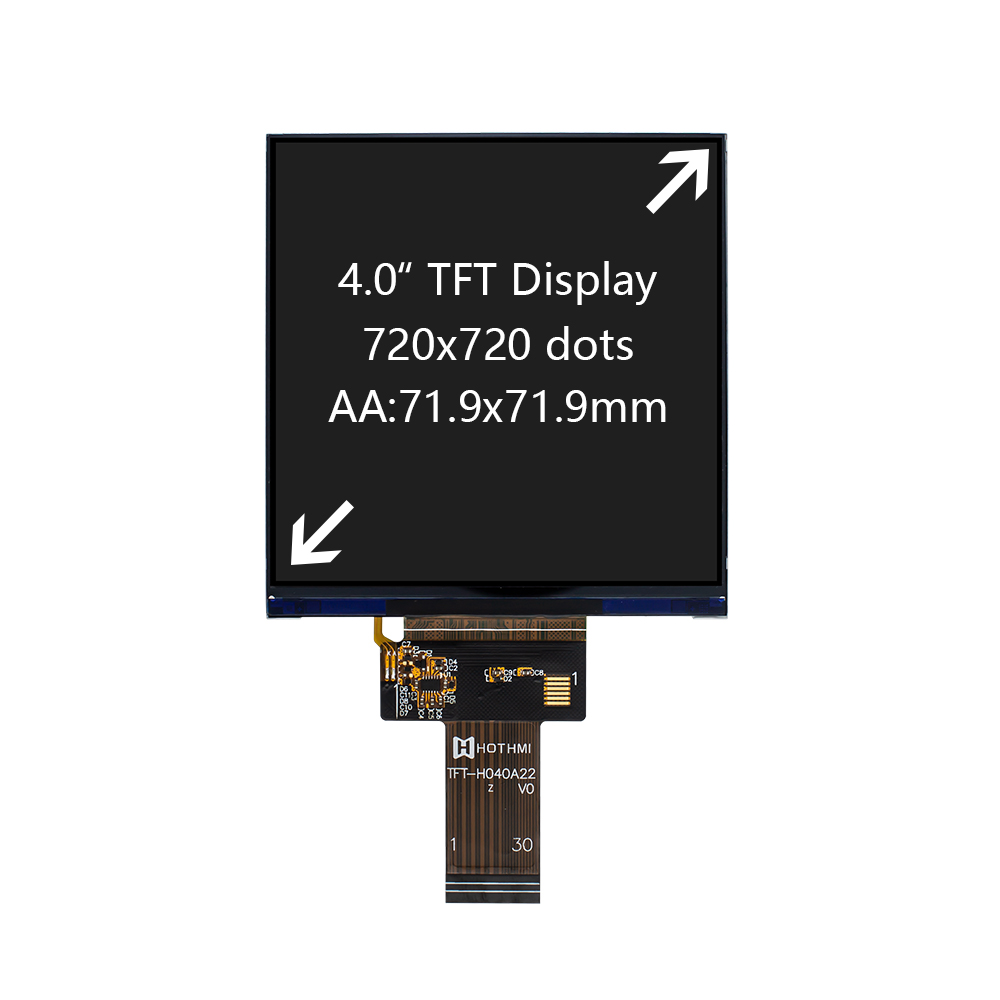
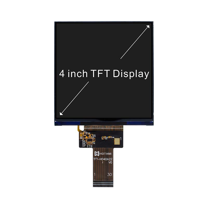
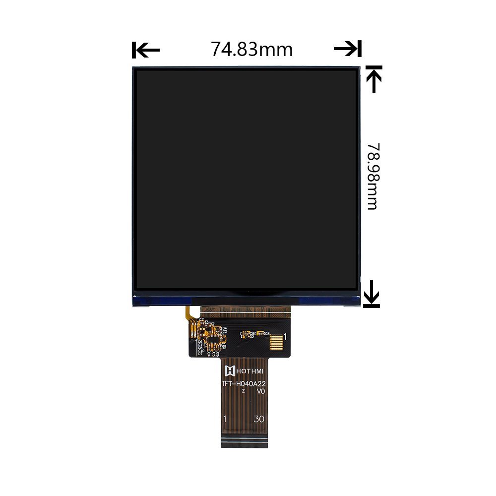
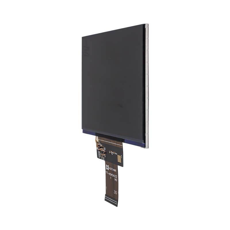
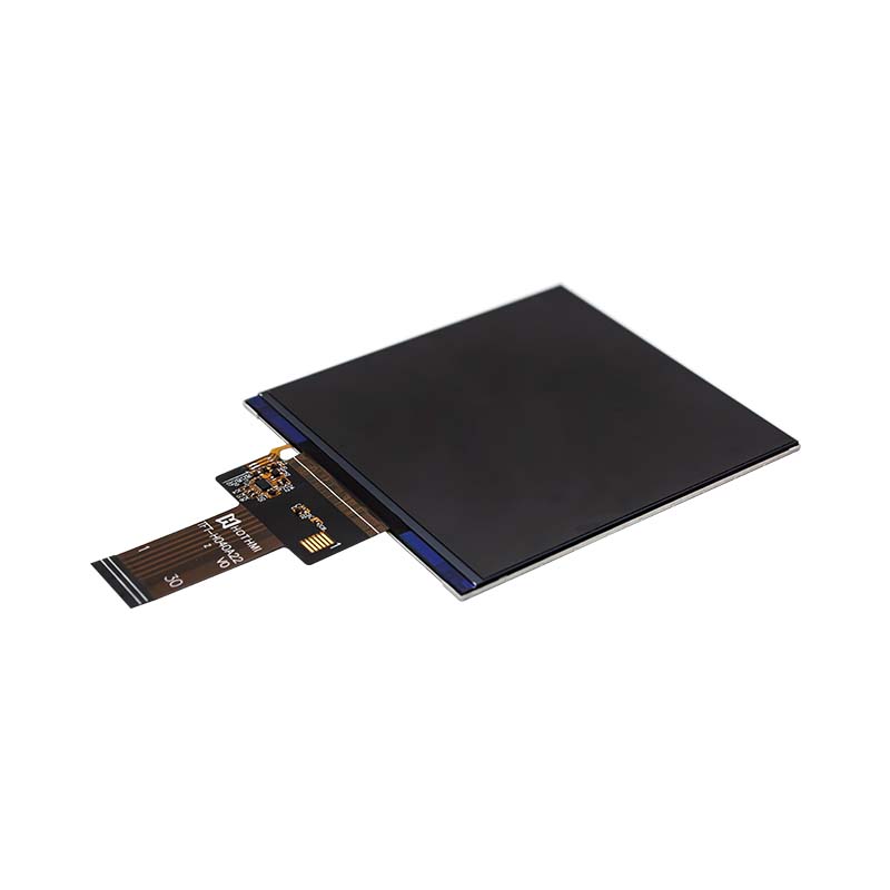
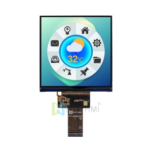
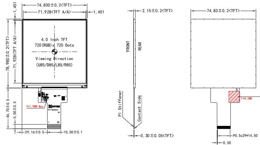
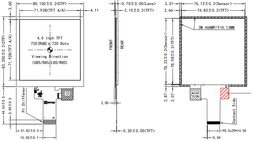
LVDS Screen is a 4.0-inch TFT LCD display with a resolution of 720(RGB)×720 pixels and a 1:1 display aspect ratio. It adopts a transmissive normally black display mode, supports 16.7M colors, and offers a viewing angle range of U85/D85/L85/R85 (full viewing angle). The operating voltages are VCI=3.3V and VDD=3.3V (typical values). The LVDS Screen operating temperature ranges from -30°C to 80°C, and the storage temperature is also -30°C to 80°C. The driver IC is ST7701S or a compatible chip, and the interface type is LVDS + 3SPI. For backlight driving conditions, the typical VF ranges from 11.2V to 13.6V with IF=40mA, and the typical module brightness is 300 cd/m².
None touch version:
Capacitive touch version:
Core Highlights of LVDS Screen
- 1:1 golden ratio high-definition square screen: This LVDS Screen features a unique 720×720 resolution specifically designed for knob screens, smart control panels, and high-end musical instrument displays, offering better visual impact and space utilization than traditional 4:3 or 16:9 screens.
- High-speed LVDS and 3SPI composite bus: Uses 3-wire SPI to write initialization commands and LVDS to transmit full-color images. The differential signal mechanism ensures stable high refresh rates above 60Hz even in harsh environments with long cables and high electromagnetic interference (EMI).
- Industrial-grade wide temperature operation standard: The module uses wide-temperature LCD materials and high-weatherability packaging processes. Both the operating and storage temperature ranges span from -30°C to +80°C, enabling stable operation in extreme cold or continuously hot industrial environments.
- Cost-effective backlight solution: Provides 300 cd/m² (typical) industrial balanced brightness. While ensuring clear visibility indoors and in semi-outdoor environments, it reduces the backlight driving voltage to 11.2V to 13.6V, significantly lowering overall power consumption and heat generation.
Pin Description and Interface Wiring of the LVDS Screen
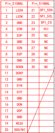
Physical Interface Definition (30-Pin Interface List)
The TFT-H040A22DKINV3N30 LVDS Screen display module connects to the main control board via a 30-pin gold finger flexible printed circuit (FPC) with a pin pitch of 0.5mm. The pins highly integrate LVDS differential pairs, SPI configuration bus, capacitive touch I2C, and backlight power lines. The following is a detailed physical pin electrical definition and function analysis.
Backlight and Electrical Characteristics of the LVDS Screen
System Operating Voltage
The LVDS Screen module’s chip and digital interface are driven by a standard 3.3V logic voltage:
- Analog supply (VCI): Typical value 3.3V.
- Digital supply (VDD): Typical value 3.3V.
Backlight Electrical Specifications and Driving Guidelines
To ensure long-term stable operation and maintain the standard industrial brightness of 300 cd/m², hardware engineers must follow these backlight driving specifications:
- Drive mode: Must use constant current drive solution. Direct connection to a constant voltage source is strictly prohibited.
- Forward voltage (VF): Typical range is 11.2V to 13.6V.
- Forward current (IF): Fixed current test standard is 40mA.
- Recommended dimming circuit: It is recommended to use a single-chip boost constant current IC (such as LP3352) and connect the 25KHz PWM signal output from the host controller to the DIM pin of the driver IC to achieve 0% to 100% flicker-free smooth dimming.
Target Applications of the LVDS Screen
Thanks to the high-speed differential anti-interference characteristics of the LVDS Screen, the 1:1 golden ratio square screen, and industrial-grade wide temperature performance, the TFT-H040A22DKINV3N30 is widely deployed in the following industries:
- Smart home touch knobs and control panels: High-end wall-mounted smart control panels, full-color touch multifunction displays for blenders/ovens with square shapes. The full-viewing-angle IPS technology ensures users can accurately read interface parameters from any squatting or side-viewing angle.
- Industrial instruments and testing terminals: Network analyzer panels, high-precision digital oscilloscopes, power environment monitoring gateways. The LVDS differential signal mechanism makes it immune to EMI interference from high-voltage inverters and strong electromagnetic workshops.
- Professional audio/musical instrument displays: High-end electric piano control panels, digital mixing console status displays. The square screen’s compact geometry efficiently arranges multi-track audio waveform graphs.
Technical FAQ for LVDS Screen
Q1: Why choose the LVDS + 3SPI composite interface for this 4.0-inch screen? What is the difference from pure SPI or pure RGB interfaces?
A1: Traditional 4.0-inch low-resolution screens often use pure SPI (slow speed, low refresh rate) or RGB interfaces (occupying over 20 pins, poor anti-interference, difficult to route with equal length). This module has a high 720×720 resolution (total pixel count up to 518,400 pixels). If driven by pure serial SPI, limited by single-line bandwidth, refreshing one frame would take an extremely long time, resulting in catastrophic lag.
Therefore, the module creatively applies the LVDS Screen composite interface:
the 3-wire SPI interface (pins 21, 22, 23) is used only during system power-on to lightly initialize the ST7701S driver chip’s registers, Gamma curve, and resolution format.
After configuration, the high-speed LVDS differential bus carries the massive pixel rendering image signals for long-distance, high-speed transmission via low-amplitude differential pairs. This not only maximizes the host controller’s data throughput to maintain a smooth 60Hz refresh rate but also provides unparalleled ultra-strong anti-EMI capability.
Q2: Why do I see inverted colors, severe color distortion, or left-right image mirroring when testing LVDS video signals?
A2: This is usually because the LVDS signal format output by the host controller (such as VESA standard vs. JEIDA standard) does not match the default demodulation format of the screen-side driver chip, or because the differential pair physical wiring order is crossed.
According to the specification sheet, the module’s LVDS data format, bit width (supports 6-bit/8-bit), channel sequence, and polarity can all be freely swapped and modified via software code.
First, no need to change PCB routing; directly read and write the specific format control registers of the ST7701S (such as the LVDS_POL polarity bit and CH_SWAP channel mapping bit in the registers) via the 3-wire SPI bus.
Then, compare with the host controller’s LVDS output pin mapping (Data 0 to 3 corresponding to P/N) and modify the soft polarity of corresponding channels in the software driver source code to correct inverted or misaligned images to normal full-color display at zero cost and high efficiency.
Q3: Why does the screen occasionally flash white light at power-on, or why does the capacitive touch screen probabilistically become unresponsive?
A3: These issues are usually caused by two hardware design flaws.
White flash: The ST7701S needs time to load registers. If backlight power is pulled high too early at power-on, liquid crystal molecules haven’t reached the initial blanking state, causing an instantaneous white flash.
Correct procedure: After host power-on, perform a hardware reset via RESX and write full initialization parameters via 3-wire SPI. Then delay 120ms to allow system power to stabilize and frame memory to be established. Finally, supply LEDA/LEDK power via the EN pin of the backlight driver IC. This achieves a seamless “black screen elegant startup”.
Touch unresponsiveness: The CTP I2C signal lines must use pull-up resistors of 2KΩ to 4.7KΩ. If resistors are too high (e.g., 10KΩ), waveforms distort under strong EMI, causing communication handshake failure between host and touch IC. Verify the measured resistance on the main control board falls within this range.
If you have any other needs, please contact us.